Electronics Conquered New Heights: Scientists Stacked Six CMOS Transistors on Top of Each Other for the First Time
Researchers from King Abdullah University of Science and Technology (KAUST) have developed the world's first six-level hybrid CMOS circuit, setting a new record in chip manufacturing. This breakthrough triples the previous record held by Belgium's Imec center, offering a new path to overcome the physical limitations of traditional chip design.
Why Vertical Stacking Matters
The demand for low-power, flexible, and scalable integrated circuits is surging. However, traditional horizontal chip layouts are hitting a wall due to resolution and cost constraints. As detailed in Nature Electronics, vertical integration, or 3D stacking, addresses these challenges by:
- Increasing transistor density on the same footprint.
- Shortening the connections between components.
- Minimizing signal delays and parasitic effects.
- Enabling low-temperature manufacturing, which is critical for preventing overheating in dense, multi-layered chips.
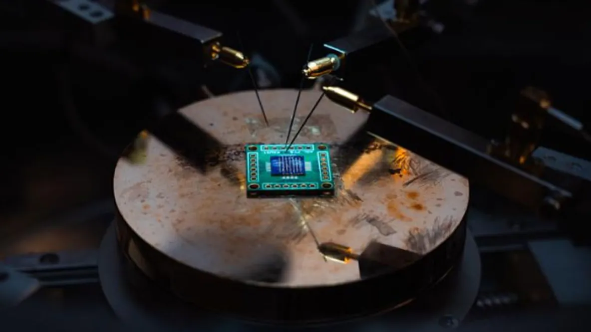
Previous efforts were limited to two layers due to challenges with alignment and overheating. This new platform overcomes those barriers, demonstrating a record-breaking six transistor stacks with 41 technological layers.
The 6-Level Innovation
The innovative design combines n-type oxide thin-film transistors (OxTs) with p-type organic thin-film transistors (OrTs), making it ideal for mass-producing next-generation electronics like flexible displays, wearable sensors, and IoT devices.
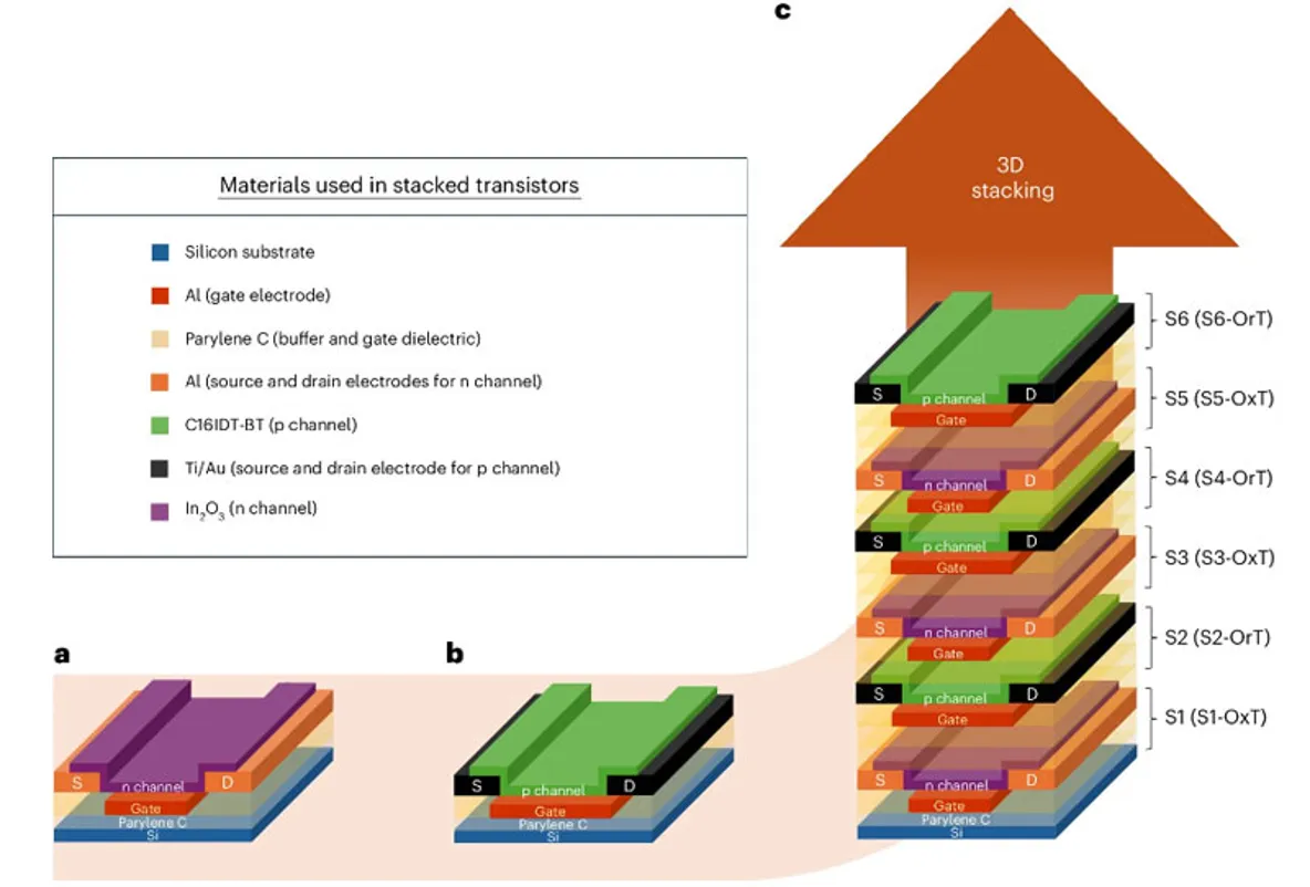
The structure was fabricated using a sophisticated 40-step lithographic process on silicon wafers. Key to their success was a low-temperature approach, where the entire process was kept at room temperature or did not exceed 100°C. This prevented thermal damage to the underlying layers, a major hurdle in previous multi-layer designs.
Impressive Performance Metrics
Testing across 600 devices confirmed the design's effectiveness. Experimental hybrid inverters built from the arrays demonstrated:
- A maximum gain of 94.84 V/V.
- A low power consumption of just 0.47 µW.
- A stable switching voltage between 0.93V and 2.61V.
Logic gates, including NOR gates, built with the six-level transistors were also successfully tested, validating the platform's potential for complex computations.
The Future of High-Density Electronics
This platform paves the way for creating highly dense, energy-efficient circuits that significantly outperform previous designs. The low-temperature process also ensures compatibility with flexible substrates, opening up new possibilities for advanced logic, memory, and sensors that could revolutionize energy-efficient technology. The team's next steps involve optimizing the upper layers and scaling the process for larger substrates, bringing this groundbreaking technology closer to commercial reality.